Description
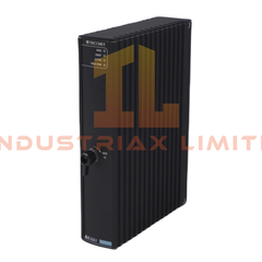
Yokogawa SDV541 Digital Output Module
The Yokogawa SDV541-, also cataloged as the SDV541 Digital Output Module, operates as a discrete output interface component for electrical load switching within Yokogawa distributed control system (DCS) I/O architectures. Configured for relay-based digital actuation in field termination assemblies, the Yokogawa SDV541- (SDV541 Digital Output Module) provides direct electrical switching via Form A relay contacts for controller-to-field device execution.
Suffix Breakdown & Model Matrix
-
SDV541: Base digital output module designation
-
No additional suffix decoding information provided in source data
-
Electrical configuration fixed to Form A relay output architecture
Hardware Specifications
| Parameter |
Specification |
| ModelBrand |
Yokogawa SDV541- |
| Origin |
Japan |
| Weight |
0.4 kg |
| Dimensions |
120 mm (W) x 93 mm (H) x 29 mm (D) |
| OperatingTemp |
-20 degC to +70 degC |
| PowerConsumption |
Not specified (system rack dependent) |
| Channels |
8 isolated output channels |
| Output Type |
Form A (NPN relay contact) |
| Output Load |
250 VAC, 5 A |
| Input Voltage |
24 VDC +/-10 percent |
Channel-to-Channel Isolation and DCS Output Architecture
The SDV541 output stage is structured around channel-separated relay elements designed for discrete load segmentation within Yokogawa CENTUM I/O subsystems. Each channel operates as an independent switching node, allowing distributed actuation without shared conductive output paths between channels.
In DCS digital output topology, relay-based Form A execution provides galvanic separation between control logic and field switching circuits. The module’s 24 VDC supply domain is internally decoupled from the relay switching elements, supporting deterministic ON/OFF state propagation under scan-cycle driven control logic. Output contact wear characteristics are defined by mechanical relay actuation limits rather than semiconductor switching degradation profiles.
Frequently Asked Questions
Q: Can the SDV541 module outputs be hot-swapped under load conditions?
A: Hot-swap behavior depends on system rack implementation. Relay contacts should not be switched under high inrush load conditions without external suppression.
Q: Are all 8 channels electrically independent?
A: Each channel is implemented as an individual Form A relay contact; however, isolation level is constrained by internal module design and backplane grounding scheme.
Q: Does the module support DC inductive load switching directly?
A: Inductive loads require external flyback suppression (diode or RC snubber) to prevent contact erosion and arcing.
Field Installation Guidelines
Mount the module into a compatible Yokogawa I/O rack backplane ensuring full seating of the edge connector. Maintain separation between field wiring and control wiring to reduce inductive coupling on relay output lines. For inductive or high inrush loads, install external suppression networks directly at the field terminal side. Shielded cabling is recommended for long run outputs, with shield termination performed at a single earth reference point within the cabinet. Ensure all 24 VDC supply wiring complies with panel grounding and isolation rules defined for DCS I/O power domains.