Description
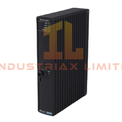
Yokogawa SDV531-S53 Digital Output Module
Configured for discrete signal actuation in DCS output subsystem execution within Yokogawa CENTUM-style control architectures, the Yokogawa SDV531-S53 (SDV144 Digital Output Module) provides direct physical/electrical execution of 24 V DC current-sourcing switching commands to field actuators and interposing relays.
Suffix Breakdown & Model Matrix
SDV531-S53 model designation is provided as a fixed ordering code. No validated sub-variant decomposition beyond manufacturer suffix definition is available from supplied data.
Hardware Specifications
| Parameter |
Specification |
| ModelBrand |
Yokogawa SDV531-S53 |
| Origin |
Not specified |
| Weight |
1 kg |
| Dimensions |
10.7 cm x 13 cm x 3.2 cm |
| OperatingTemp |
-20 degC to 70 degC |
| PowerConsumption |
Not specified |
| Output Channels |
8-channel |
| Output Voltage |
24 V DC |
| Output Type |
Current source |
| Output Response Time |
30 ms max |
| Isolation |
Module isolation |
Channel Isolation and DCS Output Architecture
The SDV531-S53 implements channel-to-channel isolation within an 8-point discrete output structure, reducing cross-channel electrical interference during simultaneous switching events. Within Yokogawa DCS environments, the output stage is designed for direct load energization at 24 V DC sourcing mode, supporting deterministic actuation timing with a maximum response latency of 30 ms. Isolation architecture is aligned with process control backplane segmentation practices typical of Yokogawa field I/O subsystems.
Frequently Asked Questions
Q: Can the SDV531-S53 outputs be hot-swapped under load conditions?
A: Hot-swap capability is not specified. In standard DCS practice, output modules require de-energized field loops prior to insertion or removal.
Q: Does each channel share a common reference or maintain full isolation?
A: The module is specified with channel isolation at module level. Field wiring design should still assume appropriate grouping of return paths unless system documentation states full per-channel isolation.
Q: What is the switching delay behavior under full channel utilization?
A: Output response time is specified up to 30 ms maximum; timing is not reported as load-dependent in the provided dataset.
Field Installation Guidelines
Ensure 24 V DC field power is verified before termination of output wiring. Maintain correct polarity for current-sourcing outputs and avoid mixing inductive loads without appropriate suppression elements such as flyback diodes or snubber circuits. Shielded cable grounding should be terminated at a single instrument earth point to minimize noise coupling into adjacent I/O channels. Maintain minimum separation between power and signal wiring within the cabinet to reduce switching transient interference.