Description
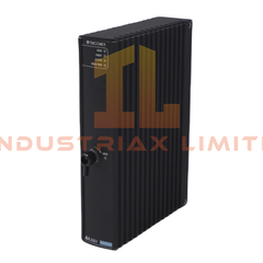
Yokogawa SDV531-L63 Digital Output Module
Configured for discrete output execution in distributed control systems (DCS) I/O sub-systems, the Yokogawa SDV531-L63 (SDV531-L63 Digital Output Module) provides direct physical/electrical execution for 8-channel 24 VDC switching control within Yokogawa field I/O architectures.
Suffix Breakdown & Model Matrix
Not applicable: SDV531-L63 is a fixed model designation without disclosed hierarchical suffix segmentation in the provided specification.
Hardware Specifications
| Parameter |
Specification |
| ModelBrand |
Yokogawa SDV531-L63 |
| Origin |
JAPAN |
| Weight |
0.3 kg |
| Dimensions |
Not specified |
| OperatingTemp |
-20 to 70 degC |
| PowerConsumption |
External supply 24 VDC, min 5 A (system level) |
| Output Channels |
8 channels |
| Output Type |
Current source digital output |
| Output Voltage |
24 VDC |
| Voltage Drop |
Max 1 V |
| Max Load Current |
0.6 A per channel (total 4.8 A) |
| Leak Current |
Max 1.6 mA |
| Response Time |
Max 30 ms |
| Withstand Voltage |
2 kVAC, 1 min (signal to system) |
| Load Resistance Range |
40 to 685 ohm |
| Minimum Load Current |
35 mA |
Channel Isolation and Backplane Execution Behavior (Yokogawa DCS I/O Architecture)
The SDV531-L63 integrates into Yokogawa I/O backplane structures with channel-level output segregation supporting controlled switching of 24 VDC field devices. Output stages operate as current source drivers with defined leakage limits (1.6 mA max), enabling stable OFF-state discrimination under partial load conditions. Signal conditioning and isolation design aligns with distributed module segmentation practices, reducing cross-channel electrical interaction during simultaneous switching events. Response timing is constrained to 30 ms maximum per output transition, reflecting deterministic scan-to-field propagation within the I/O subsystem.
Frequently Asked Questions (FAQ)
Q: Does SDV531-L63 support hot-swap replacement while field power is present?
A: Hot-swap capability depends on system rack configuration. Electrical output terminals must be de-energized to prevent backfeed into active loads.
Q: What is the impact of exceeding per-channel load current limits?
A: Exceeding 0.6 A per channel may result in output stage voltage drop increase beyond 1 V and potential protective shutdown or degradation of switching integrity.
Q: Can outputs be paralleled for higher current drive?
A: Parallel operation is not supported at channel firmware or hardware design level; each channel operates as an independent current source output stage.
Field Installation Guidelines
Maintain segregation between field wiring and control wiring to minimize coupling on 24 VDC output lines. Use shielded cabling with single-point grounding at cabinet earth reference. Ensure each output channel load remains within specified resistance range (40 to 685 ohm) to maintain valid switching behavior. Terminal torque and connector seating must comply with rack-specific mechanical standards to avoid intermittent contact resistance. Verify isolation integrity between signal lines and system ground prior to energization (2 kVAC withstand specification boundary).