Description
Yokogawa SDV531-L33 Digital Output Module
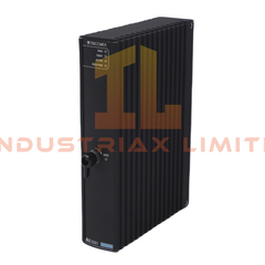
The Yokogawa SDV531-L33 also cataloged as the SDV531-L33 Digital Output Module, operates as a dedicated hardware component for discrete signal actuation within Yokogawa distributed control system I/O subsystems. It provides direct electrical switching via isolated solid-state relay outputs for field device control.
Suffix Breakdown & Model Matrix
Model designation SDV531-L33 is treated as a single fixed ordering code. No validated manufacturer-published segmentation for suffix fields is available in the provided dataset. Functional interpretation remains tied to SDV500-series digital output architecture only.
Hardware Specifications
| Parameter |
Specification |
| Model |
Yokogawa SDV531-L33 |
| Origin |
Japan |
| Weight |
Not specified |
| Dimensions |
Standard Yokogawa rack module form factor (exact values not provided) |
| OperatingTemp |
0 degC to 60 degC |
| PowerConsumption |
5 W typical |
| Output Channels |
16 channels digital output |
| Output Type |
Solid-state relay outputs |
| Rated Voltage |
24 VDC |
| Output Current |
Max 0.5 A per channel |
| Isolation |
Channel-to-channel isolation |
| Diagnostics |
Short-circuit detection, open-load detection |
Channel-to-Channel Isolation and Output Execution Logic
The SDV531-L33 implements per-channel galvanic separation within the output stage to reduce inter-channel electrical coupling during simultaneous switching events. In Yokogawa DCS I/O topology, discrete output activation is executed through backplane command framing followed by transistor-level switching of 24 VDC loads. Diagnostic feedback loops monitor load continuity and fault states such as open-circuit or short-circuit conditions at the field termination layer.
FOUNDATION Fieldbus / PROFIBUS PA integration is not native to this module; it operates as a direct digital output node within the central I/O rack architecture, relying on system-level communication through the Yokogawa control bus rather than field-level protocol embedding.
Frequently Asked Questions
Q: Can the SDV531-L33 channels be hot-swapped under load conditions?
A: Module replacement is dependent on system rack configuration. Field wiring must be de-energized prior to removal to prevent output stage stress and backfeed conditions.
Q: What is the backplane impact of all channels switching simultaneously?
A: Backplane load is governed by module power consumption (5 W typical) and does not scale linearly with channel switching, as output switching is performed at field-side transistor stages.
Q: Does the module support mixed voltage outputs per channel?
A: No. All channels are referenced to a unified 24 VDC output architecture with shared system potential structure and channel isolation.
Field Installation Guidelines
Maintain separation between field wiring and communication backplane conductors to reduce electromagnetic coupling. Ensure correct torque application on terminal blocks per Yokogawa rack assembly standards. Shield termination should be grounded at a single point on the cabinet earth bar to avoid ground loop formation across isolated output channels. Verify load impedance compatibility before energizing outputs to prevent sustained short-circuit diagnostic lockout conditions.