Description
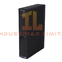
Yokogawa ADV561P00S2 Digital Output Module
TheYokogawa ADV561P00S2serves as the primaryADV561P00S2 Digital Output Module utilized to execute discrete field device switching across CENTUM VP I/O subsystem platforms. Configured for transistor-based current sink output operation in a 24 VDC load environment, the module provides 64-channel digital output control with defined low-level output saturation behavior and integrated status feedback handling.
Suffix Breakdown & Model Matrix
No validated suffix segmentation is defined in the provided technical data for ADV561P00S2. The full model string is treated as a single ordered part number.
Hardware Specifications
| Parameter |
Specification |
| ModelBrand |
Yokogawa ADV561P00S2 |
| Origin |
JAPAN |
| Weight |
0.3kg
|
| Channel Count |
64 digital output channels |
| Output Type |
Transistor current sink |
| Rated Load Voltage |
24 VDC |
| Output ON Voltage Drop |
Max 2 VDC |
Yokogawa Field I/O Signal Conditioning and Channel Architecture
Within Yokogawa Field I/O architectures, the ADV561 series implements transistor-based switching elements optimized for discrete signal interfacing with field actuators. Channel-to-channel electrical isolation architecture is applied at the module backplane interface level, supporting deterministic ON/OFF state execution with minimized leakage current propagation across adjacent output channels. The design aligns with DCS-level digital signal conditioning requirements where stable sink-current behavior is required under 24 VDC load distribution networks.
Frequently Asked Questions
Q: Can the ADV561P00S2 outputs be hot-swapped under load conditions?
A: Hot-swap capability is dependent on CENTUM VP base unit configuration. Field wiring must be de-energized prior to module insertion or removal to avoid transient backfeed into transistor output stages.
Q: What is the electrical behavior during output OFF state?
A: In OFF state, output transistors present high impedance with leakage current limited by internal suppression circuitry, maintaining isolation from 24 VDC load rails.
Q: Does channel activation introduce measurable propagation delay?
A: Output response is governed by internal scan cycle timing of the I/O subsystem, typically aligned with DCS task scheduling rather than discrete hardware switching delay.
Field Installation Guidelines
The module shall be installed in a compatible Yokogawa CENTUM VP or Field I/O rack system with verified backplane alignment. Ensure that all field wiring is terminated according to current sink output topology, with proper common return routing to avoid floating reference conditions.
Shielded cables are recommended for long-distance actuator connections. Shield termination should be performed at a single-point ground reference to reduce ground loop formation across multi-channel output groups.
Backplane connectors must be fully seated without mechanical stress. Avoid applying torque or lateral force during insertion to prevent contact misalignment in the I/O rack interface.