Description
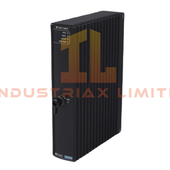
Yokogawa ADV869-P01 Digital I/O Module
The Yokogawa ADV869-P01 also cataloged as the ADV869 Digital I/O Module, operates as a dedicated hardware component for discrete signal acquisition and transistor output control within Yokogawa DCS input/output subsystems. It executes 32-channel digital input processing and 32-channel transistor output switching with defined electrical isolation every 16 channels.
Hardware Specifications
| Parameter |
Specification |
| ModelBrand |
Yokogawa ADV869-P01 |
| Origin |
Not specified |
| Weight |
Approx. 0.30 kg |
| PowerConsumption |
Max 800 mA at 5 VDC |
| Input Channels |
32-channel input |
| Output Channels |
32-channel transistor output |
| Signal Isolation |
Common isolation per 16 channels |
| Input OFF Signal |
>= 100 kOhm |
| Input ON Signal |
<= 200 Ohm |
| Input Voltage Range |
OFF: 4.5 to 25 VDC; ON: <= 1 VDC |
| Output Rating |
30 VDC, 100 mA (resistive/inductive) |
| Response Time |
Input: 8 ms; Output: <= 16 ms |
| Pulse Width |
8 ms to 7200 s |
Channel-to-Channel Digital Isolation and DCS Scan Handling
The ADV869-P01 implements grouped electrical isolation across 16-channel blocks, reducing cross-channel interference during simultaneous switching events. Within Yokogawa DCS architectures, input scanning is synchronized to backplane polling cycles, ensuring deterministic state acquisition for discrete field signals. The transistor output stage supports inductive load switching with controlled response timing up to 16 ms, enabling stable actuation of relays and solenoid interfaces. Pulse width configuration from 8 ms to 7200 s allows timed control execution directly at module level without external sequencing logic.
Frequently Asked Questions
Q: Can the ADV869-P01 support hot-swapping during operation?
A: Hot-swap capability depends on the host rack design. Electrically, the module uses backplane-driven power (5 VDC), and removal under load may interrupt I/O scanning cycles.
Q: What is the channel isolation structure of this module?
A: Isolation is implemented in groups of 16 channels, meaning each block shares a common reference rather than full per-channel isolation.
Q: Does the output stage support inductive load suppression internally?
A: The module supports inductive load switching at 30 VDC, 100 mA; external suppression (flyback diode or snubber) is typically required for extended contact life.
Field Installation Guidelines
Install the module into a compatible Yokogawa I/O rack with backplane alignment fully seated before applying 5 VDC system power. Ensure field wiring is segregated between input and output terminals to prevent coupling on shared signal commons. For inductive loads, install external suppression devices directly at the load terminals. Maintain proper grounding of the rack chassis to minimize noise on low-level digital input detection thresholds.