Description
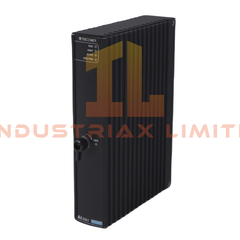
Yokogawa ADV859-P00 Digital I/O Module
Configured for isolated 16-channel discrete signal handling in CENTUM-compatible control networks, the Yokogawa ADV859-P00 (ADV859 Digital I/O Module) provides direct physical/electrical execution for contact status acquisition and transistor output switching through ST2-compatible card architecture.
Hardware Specifications
| Parameter |
Specification |
| Model |
ADV859-P00 |
| Brand |
Yokogawa |
| Product Type |
Digital I/O Module |
| Input Channels |
16-channel digital input |
| Output Channels |
16-channel digital output |
| Signal Isolation |
Isolated channels |
| Input Signal Type |
Contact input, voltage input |
| OFF Signal Detection |
100 kOhm or more |
| ON Signal Detection |
200 Ohm or less |
| Minimum Current for Short-Circuited Contact |
1.25 mA |
| Voltage Input OFF Signal |
4.5 to 25 VDC |
| Voltage Input ON Signal |
+/-1 VDC, 200 Ohm or less |
| Input Contact Rating |
5 VDC, 20 mA or more |
| Pushbutton Input Function |
Not supported |
| Input Response Time |
8 ms |
| Output Signal |
Transistor contact |
| Output Contact Rating |
30 VDC, 100 mA |
| Supported Load Type |
Inductive load, resistive load |
| Output Response Time |
16 ms or less |
| Pulse Width Range |
8 ms to 7200 s |
| Pulse Width Resolution |
8 ms |
| ON/OFF Delay Addition |
Maximum 1 ms |
| Maximum Current Consumption |
450 mA at 5 VDC |
| External Connection |
Dedicated KS2 cable |
| Compatible Card Type |
ST2 compatible |
| Weight |
Approx. 0.30 kg |
| Origin |
Japan |
| Operating Temp |
Not specified |
| Dimensions |
Not specified |
| Power Consumption |
450 mA at 5 VDC |
Channel-to-Channel Isolation Characteristics
The ADV859-P00 implements isolated input and output channel architecture for discrete signal segregation within distributed control system environments. The module accepts both dry-contact and voltage-driven status inputs while maintaining electrical separation between field-side signal transitions and internal logic processing circuits.
Voltage input recognition is processed through defined OFF-state and ON-state thresholds to prevent false state transitions caused by line leakage or induced noise. Transistor output stages are configured for low-current DC switching with compatibility for resistive and inductive field loads up to 30 VDC.
The module interfaces through dedicated KS2 cabling and operates as an ST2-compatible card for Yokogawa control platform integration.
Frequently Asked Questions
Q: Does the ADV859-P00 support hot-swapping during system operation?
A: The supplied specification does not explicitly define online insertion or removal capability. Module replacement procedures should follow the host DCS cabinet maintenance sequence and controller isolation practices.
Q: What type of field devices can be connected to the digital outputs?
A: The transistor outputs support inductive and resistive DC loads rated up to 30 VDC and 100 mA per output point.
Q: Can the module accept both contact and voltage-based digital inputs simultaneously?
A: The module supports both contact input and voltage input detection methods according to the specified ON/OFF threshold conditions.
Field Installation Guidelines
-
Use shielded field wiring for digital input circuits routed near inverter, relay, or motor starter cabling.
-
Separate input and output wiring bundles to reduce transient coupling between switching circuits.
-
Verify KS2 cable connector retention before energizing the I/O rack.
-
Maintain proper DC common reference continuity between external devices and module terminals.
-
For inductive output loads, install external flyback suppression devices to limit transistor switching transients.
-
Avoid routing low-level digital signal wiring in parallel with high-current AC feeder conductors.