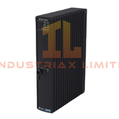
Yokogawa F3YD14-0N Digital Output Module The Yokogawa F3YD14-0N also cataloged as the F3YD14-0N Digital Output Module, operates as a dedicated...
اقرأ المزيد
متاح في أيام العمل من الساعة 9:00 صباحًا إلى 6:00 مساءً
راسلنا عبر البريد الإلكتروني: sales2@industriaxplc.com
متاح 24/7 للاستفسارات والدعم
وصف
Yokogawa F3YD14-0N Digital Output Module
The Yokogawa F3YD14-0N also cataloged as the F3YD14-0N Digital Output Module, operates as a dedicated hardware component for transistor-level discrete signal switching within the Yokogawa FA-M3 PLC system. The module executes 14-point sink-type output switching with defined current limitation and fast ON/OFF electrical response at the backplane I/O interface.
Suffix Breakdown & Model Matrix
No validated manufacturer-provided suffix segmentation for F3YD14-0N is available in the supplied dataset. No decomposition is applied.
Hardware Specifications
Parameter
Specification
Model
Yokogawa F3YD14-0N
ModelBrand
Yokogawa
Module Type
Digital Output Module (Transistor, Sink type)
Output Points
14 points per common
Rated Load Voltage
12 to 24 VDC
Max Load Current
2 A per point, 14 A per common
ON Voltage Drop
0.5 VDC max
OFF Leakage Current
0.1 mA max
Response Time
ON/OFF: 1 ms max
Power Consumption
5 VDC internal: 100 mA; external supply: 12 to 24 VDC, 10 mA
Within Yokogawa FA-M3 I/O architecture, the F3YD14-0N transistor output stage is implemented as a sink-type switching array designed for deterministic discrete control. Each channel is electrically referenced to a common potential rail, enabling controlled current sinking behavior for field loads such as relay coils, solenoid valves, and indicator circuits.
The module design aligns with DCS-class I/O segmentation principles, where output stage isolation is structured to minimize cross-channel interaction during simultaneous switching events. The internal output driver topology is coordinated with backplane communication timing to maintain stable signal state transitions under mixed inductive and resistive loading conditions.
Integration with system-level analog and communication modules in Yokogawa platforms typically follows standardized field wiring separation practices consistent with 4-20 mA loop segregation and fieldbus noise isolation design rules.
Frequently Asked Questions
Q: Can the module outputs be hot-swapped under load conditions? A: Hot-swapping is not supported under energized field load conditions. Output state must be forced to OFF and external field power removed prior to module insertion or removal to avoid driver stress.
Q: Does each output channel provide galvanic isolation? A: Channel-to-channel isolation is implemented at the driver architecture level; however, outputs share a common reference structure. Full galvanic isolation per channel is not specified.
Q: What is the impact of inductive load switching on output lifetime? A: Inductive loads are mitigated by built-in active clamp surge suppression. External flyback protection is still recommended for high-energy coils to reduce stress on switching elements.
Field Installation Guidelines
Output wiring shall be performed using shielded or routed cable harnesses with separation from analog and communication lines. Terminal tightening must follow M3.5 screw torque specifications defined by control cabinet assembly standards.
Field devices should be verified for compatible voltage range within 12 to 24 VDC before energization. Load inrush characteristics must be evaluated to ensure per-channel current does not exceed 2 A limit. Common return paths should be sized for aggregated current up to 14 A per common group.
Proper grounding of cabinet backplane and maintenance of low-impedance earth reference are required to minimize switching noise coupling into adjacent I/O modules.
تحديد
rtl">
المزايا
موثوقية عالية في البيئات الصناعية
يدعم التشغيل المستمر، متوافق مع أنظمة PLC/DCS الرئيسية